The Story of the Pixel Visual Core
A philosophical dive into Google's Pixel Visual Core — why even domain-specific architectures need general-purpose compilers
In the summer of 2016, I was an intern under Bill Mark on the Pixel Visual Core team at Google. My job was to build the first prototype C compiler for a custom image processing chip that had yet to see its first tape-out—I was writing for a machine that only existed in RTL simulations.
When I returned for a second internship in 2018, the "ghost" had become silicon, and Google had hired a full engineering team to maintain the production stack. The chip was primarily designed for computational photography and standard TensorFlow ML workloads, but I wanted to see how far we could stretch its "domain-specific" boundaries. I proposed implementing Lattice Regression—a complex, high-dimensional machine learning model—to see if we could turn this bespoke image processor into a general-purpose AI engine.
That experiment, and the intricate virtual instruction sets we had to invent to make it work, were captured in a paper we called "Assessing New Workloads on Existing Accelerators". It was ultimately never published, and to this day, public documentation on the Visual Core completely omits the existence of our C/C++ compiler. But those missing pages contain a vital lesson: building the hidden, low-level tooling for that chip challenged everything I thought I knew about domain-specific architectures and hardware acceleration.
The Phantom Hardware
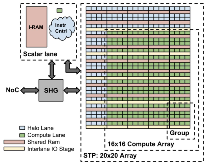
The "ghost" in question was the Pixel Visual Core (PVC)—Google's first custom-designed, fully programmable image, vision, and AI co-processor for mobile devices, which would eventually make its debut in the Pixel 2.
Under the hood, the PVC was a System-in-Package (SiP) that featured a standard ARM Cortex-A53 core for orchestration, flanked by a ring of custom-designed Image Processing Unit (IPU) cores. The IPUs used a VLIW processor architecture, with multiple data movement, scalar, and vector instructions in each bundle. As described in Jason Redgrave's 2018 HotChips presentation, the term "vector" here is misleading - it was really a 16x16 compute matrix, overlaid on a 20x20 storage matrix.
This design was meant to accelerate 3x3-5x5 stencil computations -- the most common in image processing at the time. By shifting the weight matrix around, we could easily compute the 2D convolution of common filters.
Built as a domain-specific accelerator (DSA) for computational photography, it even featured in Hennessy, Patterson, and Kozyrakis's Computer Architecture, 7th Edition as a textbook example of using domain-specific languages (like Halide) for domain-specific accelerators.
However, from my perspective down in the trenches, the textbook misses a crucial piece of the puzzle.
The Captive Audience (The Missing Piece)
One of the claims in Hennessy, Patterson, and Kozyrakis's 7th Edition -- specifically Chapter 7, section 2 -- asserts:
5. Use a domain-specific programming language to write code for a DSA. As Section 7.1 mentions, a classic challenge for DSAs is getting applications to run on your novel architecture. A long-standing fallacy is the assumption that your new computer is so attractive that programmers will rewrite their code just for your hardware. Fortunately, domain-specific programming languages and libraries were becoming popular even before architects were forced to switch their attention to DSAs. [...] They make porting applications to your DSA much more feasible.
This statement is broadly true. If you make a domain-specific accelerator, you should expect second-party and third-party users to interact with it via a domain-specific language like Halide or TensorFlow.
However, having been tasked with building the foundational C compiler, I saw firsthand a crucial dynamic the textbook glosses over: your new computer has an audience, albeit a captive one—your first-party compiler and applications teams.
It is unreasonable to expect backend engineers to bootstrap from a high-level DSL, analyze a suboptimal binary or a mysterious system crash, and then somehow reverse-engineer the correct sequence of target instructions. The compiler team cannot simply rely on the DSL; they are fundamentally tasked with making the DSL functional in the first place.
In practice, the way you build a compiler for these accelerators is actually quite straightforward: you start by building a bottom-level assembler and manually "playing around" with it. You work through specific examples, hand-writing the assembly until you have a rock-solid idea of the exact instruction sequences you want to generate. Only once you've felt the hardware's constraints in your own hands do you start building upward—generalizing that manual logic into an automated compiler.
This is why a bare-bones assembler and runtime is a non-negotiable requirement for any nontrivial DSA. Even if there is no "business" case for external developers to write assembly, your internal engineering velocity depends on it.
Once you have that foundational assembler, you can begin building upward into an Abstract Assembler—a thin, ergonomic layer that retains the raw expressive power of the hardware while stripping away the cognitive load of manual register scheduling. For the Pixel Visual Core, we chose a subset of C/C++ backed by LLVM to serve as this layer. For more exotic architectures, this is where modern toolchains like MLIR shine—providing the scaffolding to build domain-specific IRs without having to reinvent the wheel.
The Tale of Three ISAs: Physical, Logical, and Virtual
To build that abstract assembler, we had to grapple with the reality of how the chip actually executed code. Our compiler didn't just target one instruction set—it ultimately dealt with three distinct ISAs, each serving a crucial philosophical and practical role.
First was the Physical ISA (PISA): the raw hardware instructions natively executed by the chip. Like most VLIW architectures, the PISA was incredibly powerful but notoriously difficult to schedule and manage directly.
To make this programmable, we introduced the Logical ISA (LISA), an abstraction layer sitting directly on top of the physical hardware. One of our major goals for the LISA was to insulate the upper compiler stack from generational changes in the hardware. Admittedly, since I designed it alongside the first tape-out in 2016, this insulation was a philosophical exercise at best—there wasn't yet a second generation of the chip to verify it against!
The relationship between LISA and PISA offers a fascinating philosophical perspective. It mirrors the dynamic between Nvidia's PTX (Parallel Thread Execution) virtual ISA and its SASS (Streaming Assembly) physical ISA, or how modern x86 processors rely on microcode to translate complex instructions into underlying RISC micro-ops. The fundamental difference is simply when the translation occurs. Hardware microcode decoding and compiler lowering are functionally identical operations—by translating LISA to PISA in the compiler, we merely shifted the complexity of instruction decoding from runtime silicon to compile-time software.
Finally, we had to solve the Instruction Memory Wall. The Visual Core was originally optimized for computational photography and simpler ML operations, where kernels are relatively simple—a few dozen instructions to compute a 3x3 blur or a 5x5 Sobel filter. But our high-dimensional ML models were massive, and we couldn't just compile unrolled programs directly to the chip; they simply wouldn't fit in the IPU's tiny instruction memory.
To bypass this, we used our C/C++ compiler to build a Complex Virtual ISA (CVISA)—a virtual bytecode interpreter that sat on the chip. By treating the IPU like a virtual machine, we could ingest a high-level data stream and dispatch it to a library of highly-optimized hardware templates. To save even more space, this VM was bespoke: the compiler would only generate bytecode support for the specific CVISA instructions that were actually used by that particular application. By generating a bespoke VM tailored to each specific workload, we bypassed the chip's physical limits and executed complex programs it was never designed to hold.
In a given domain—such as lattice regression—operations like interpolations or lookups could be mapped in several optimized ways depending on their parameters (e.g., the number of weights or the size of the operation). We had to strike a delicate balance between how many of these optimized "instructions" we supported versus how highly specialized each one could be.
Because we were compiling entire applications ahead of time, we treated these operations like software templates. The compiler would analyze the application, instantiate only the highly optimized instruction blocks that were actually needed, and load only those into the limited instruction memory. We then fed the chip a data stream that acted as our runtime program, dictating jumps between these pre-compiled blocks. By generating a bespoke, application-specific instruction set, we bypassed the hardware's memory limits and executed complex programs the chip was never designed to hold.
CVISA Template Execution
1. A complex lattice regression model is too large for instruction memory.
Lattice DAG (Application)
Instruction Mem
Data Stream
Scratchpad Memory Grid
The Lookup Primitive: Bringing It All Together
The CVISA virtual machine solved our macro-level problem: fitting models with hundreds of operations into a strictly constrained instruction memory. But zooming in on a single instruction reveals the micro-level gymnastics required to make the system tick.
To understand the "complex" and "virtual" nature of these templates, consider the "lookup" primitive—a fundamental operation for evaluating lattice regression models.
Each Image Processing Unit (IPU) on the PVC didn't have a traditional cache; instead, it relied on a software-managed scratchpad memory. When we loaded a model, the compiler statically allocated space in this scratchpad to hold intermediates, the "workspace" for each CVISA instruction, and the model's weights—stored directly in the IPU's 16x16/20x20 2D "vectors." However, this 2D vector grid within the IPU was physically divided into 2x4 chunks. We only had "random" shuffle access to values within our same 2x4 chunk. If a computation needed a weight stored in a different chunk of the vector, it couldn't just read it directly.
To perform a full lookup, we had to combine group shifts to physically move these 2x4 blocks around the IPU's grid until every group could fetch its required values. This introduced a classic systems tradeoff: data replication versus storage capacity. If we heavily replicated the data across the "vectors," we needed fewer group shifts (faster lookups), but we sacrificed precious scratchpad storage space. Striking the right balance required compiling highly specialized CVISA instruction templates tailored to the exact parameters of the model.
IPU Group Shifts (No Replication)
Simulating a 20x20 data grid (10x5 chunks) with a 16x16 compute grid overlaid. We are observing a single fixed IPU group. As the data grid shifts, a new data block slides into the IPU's local memory bounds, allowing it to gather those values.
Gather Checklist
Marking off all 50 blocks as the fixed IPU observes them.
This specific primitive perfectly closes the loop on our earlier argument about Patterson and DSLs. While an end-user might happily define their lattice regression model in a high-level language like TensorFlow or Halide (or, in this case - protobuffers), you cannot write a dynamic, stateful interpreter loop—one that decodes a data stream, orchestrates complex 2x4 block shifts, and dispatches dynamic memory lookups—using a DSL meant for static feed-forward pipelines.
To build the CVISA runtime and these intricate instruction templates, we absolutely needed the expressive, low-level power of a general-purpose C/C++ compiler. This proves the point: the elegant DSL relies entirely on the systems team having the bare-metal tools required to build the virtual machine beneath it.
Implementing something as intricate as the Lookup primitive—with its 2x4 block shifts and scratchpad allocations—would have been a fool's errand if we had to wait for physical hardware or endure the glacial pace of RTL simulation to verify every cycle. On a chip where every data movement is a manual operation, the potential for "off-by-one" errors is astronomical. To survive the complexity of these high-dimensional models, we needed a way to iterate faster than the silicon would allow.
Surviving Before Silicon: The Case for a Software Simulator
The answer was a software simulator—a bit-accurate C++ model of the IPU cores that allowed us to debug our CVISA templates on ordinary workstations. To quote our (unpublished) paper:
Buggy code is a classic programming problem, usually mitigated by use of debugging environments and tools. However, on programmable accelerators the debugging utilities are never as mature and rarely as sophisticated as those for CPU toolchains. In order to alleviate this tooling gap, the group created two implementations of the Pixel Visual Core's C++ interface: one that directly wraps compiler primitives, while the other contains ordinary C++ implementations of those primitives that run on ordinary workstations using a standard C++ flow.
Relying on this "standard C++ flow" software simulator was a lifesaver for three reasons:
1. Scaling Concurrent Users: Before tape-out, RTL simulation cycles (using tools like VCS) are a precious commodity monopolized by hardware verification teams. Post-silicon, bringup teams obsess over limited engineering samples. Software, however, is infinitely scalable. With a C++ simulator, each engineer could have dozens of virtual chips at their disposal, bypassing the political crossfire over hardware allocation.
2. A Contract Between Teams: A software simulator can serve as a strict contract between software and hardware teams. Unlike x86 or ARM, which have hundreds of pages of rigorous documentation, most DSA architectures just have implementation-defined configurations. With a software simulator serving as a source of truth, semantics become well-defined. Hardware architects can sign off on unit implementations, DV can verify the RTL matches it, and compiler and application teams can have a stable surface to work from without needing to read the RTL.
3. Modern Observability: It brought the full power of software debuggers to bear. While hardware engineers spend their days staring at squiggly green lines in a waveform viewer, the software simulator gave us the full power of LLDB, print statements, and breakpoints. Using these tools, pinpointing a programming error shrinks from days to hours or minutes.

Conclusion
We achieved something definitive that summer. We showed that even the most "exotic" of architectures could be tamed with proper tooling, and that domain-specific accelerators could be leveraged far beyond their original mandate. By the end of the internship, we were performing inference on production-scale workloads in less time than it would take to ping a server over mobile data.
Hardware, like art, takes on a life of its own. Architects may design their silicon to solve one specific problem, but once it's out in the wild, the hardware becomes a blank canvas for an entirely different kind of masterpiece. The modern GPU is the ultimate example: despite its name and its roots in rasterization, the datacenter "AI accelerators" of today have evolved into dense matrix-math engines where the "Graphics" label has become a complete misnomer. We keep the name, but we use the silicon for something the original architects never envisioned—a shift so radical that flagship AI chips like the Nvidia H100 have become some of the worst "gaming" GPUs of all time.
But to discover a chip's true capabilities, you must make experimentation cheap. This is why a low-level compiler is non-negotiable. The ingredients for research are simple: grab a handful of smart people, give them the tooling to "play" with the system, and results will follow.
In our case, that rapid iteration proved that a bespoke image processor was no longer the right answer. By pushing the hardware to its limits, we inadvertently proved that our software had outgrown the architecture. The "domain" of the Pixel Visual Core had shifted from computational photography to high-dimensional AI. While the hardware briefly evolved into the Pixel Neural Core—adding an Edge TPU to handle these new workloads—the series was ultimately retired with the Pixel 5, replaced by the more general-purpose ISP and DSP blocks of the Qualcomm Snapdragon.
Looking back, one of Jason Redgrave's quips from that summer has stuck with me: "the greatest optimization a hardware engineer can make is to get rid of their own chip."
By that metric, we were brilliant hardware engineers. The Pixel Visual Core was optimized right out of existence—clearing the way for the more ambitious, system-wide integration that would eventually return in the form of the Google Tensor series. In the end, Patterson was right: the only way to scale a domain is through a domain-specific language. But our summer in the trenches proved the inverse is also true: the only way to build that language—and to discover what a piece of silicon is truly capable of—is to have the bare-metal tools required to treat it like a general-purpose machine.